Toggle light / dark theme

Despite its promising characteristics in condensed matter physics, the triply-degenerate semimetal PtBi2 has been largely unexplored in practical applications, particularly in semiconductor technology. The main difficulties include a lack of empirical data on the integration of PtBi2 with existing semiconductor components and the need for innovative approaches to leverage its unique properties, such as high stability and mobility, within the constraints of current electronic manufacturing processes.

Chinese scientists have developed a new type of lens that can be used for health care and augmented reality (AR). Based on radio frequency, the eye-tracking smart contact lenses don’t require battery or conventional silicon chips and are biocompatible and imperceptible.

Set to be used for human-machine interaction (HMI), the smart contact lenses rely on tracking eye movements. The lenses use methods like pupil center corneal reflection and electrooculography (EOG) to track eye movements.

A collaborative effort between Harvard and Google has led to a breakthrough in brain science, producing an extensive 3D map of a tiny segment of human brain, revealing complex neural interactions and laying the groundwork for mapping an entire mouse brain.

A cubic millimeter of brain tissue may not sound like much. But considering that tiny square contains 57,000 cells, 230 millimeters of blood vessels, and 150 million synapses, all amounting to 1,400 terabytes of data, Harvard and Google researchers have just accomplished something enormous.

A Harvard team led by Jeff Lichtman, the Jeremy R. Knowles Professor of Molecular and Cellular Biology and newly appointed dean of science, has co-created with Google researchers the largest synaptic-resolution, 3D reconstruction of a piece of human brain to date, showing in vivid detail each cell and its web of neural connections in a piece of human temporal cortex about half the size of a rice grain.

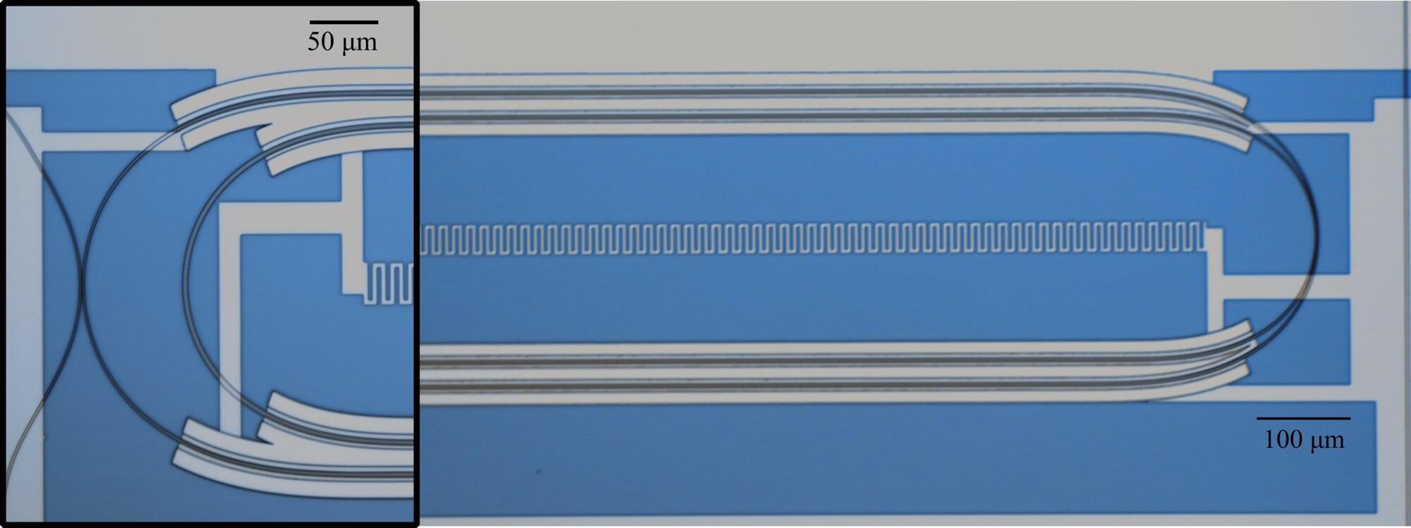
New photonic integrated circuit technology based on lithium tantalate improves cost-efficiency and scalability, making significant advancements in optical communications and computing.

Optical communications and computing systems have been revolutionized by the rapid advancement in photonic integrated circuits (PICs), which combine multiple optical devices and functionalities on a single chip.

For decades, silicon-based PICs have dominated the field due to their cost-effectiveness and their integration with existing semiconductor manufacturing technologies, despite their limitations with regard to their electro-optical modulation bandwidth. Nevertheless, silicon-on-insulator optical transceiver chips were successfully commercialized, driving information traffic through millions of glass fibers in modern data centers.

In the ongoing quest to make electronic devices ever smaller and more energy efficient, researchers want to bring energy storage directly onto microchips, reducing the losses incurred when power is transported between various device components. To be effective, on-chip energy storage must be able to store a large amount of energy in a very small space and deliver it quickly when needed—requirements that can’t be met with existing technologies.