The novel 3D wiring architecture and chip fabrication method enable quantum processing units containing 10,000 qubits to fit in a smaller space than today’s 100-qubit chips.


If quantum computing is going to become an every-day reality, we need better superconducting thin films, the hardware that enables storage and processing of quantum information. Too often, these thin films have impurities or other defects that make them useless for real quantum computer chips.
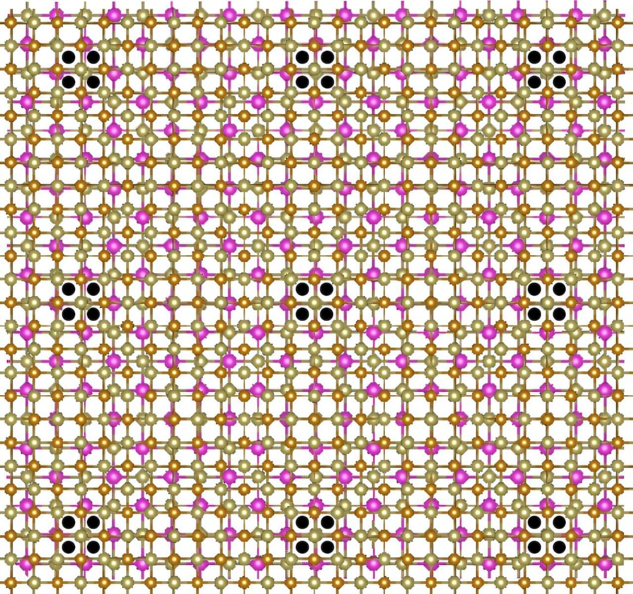
Now, Yuki Sato and colleagues at the RIKEN Center for Emergent Matter Science (CEMS) in Japan have discovered a way to make a superconducting thin film from iron telluride, which is surprising because it is not normally superconducting.
The fabrication process reduces distortion in the crystal structure, making it superconducting at very low temperatures, and thus suitable for use in quantum chips. This study was published in Nature Communications.

University of Iowa researchers have discovered a method to “purify” photons, an advance that could make optical quantum technologies more efficient and more secure.
The work is published in the journal Optica Quantum.
The researchers investigated two nagging challenges to creating a steady stream of single photons, the gold standard method for realizing photonic quantum computers and secure communication networks. One obstacle is called laser scatter, which occurs when a laser beam is directed at an atom, causing it to emit a photon, which is a single unit of light. While effective, the technique can yield extra, redundant photons, which hampers the optical circuit’s efficiency, much like a wayward current in an electrical circuit.

The bacteria in our poop are a reasonable representation of what’s living in our digestive system. To understand how different drugs can impact the gut microbiome, the team cultured microbial communities from nine donor fecal samples and systematically tested them with 707 different clinically relevant drugs.
The researchers examined changes in the growth of different bacterial species, the community composition, and the metabolome – the mix of small molecules called metabolites that microbes produce and consume. They found that 141 drugs altered the microbiome of the samples and even short-term treatments created enduring changes, entirely wiping out some microbial species. The primary force behind how the community responds to drug inhibition was competition over nutrients.
“The winners and losers among our gut bacteria can often be predicted by understanding how sensitive they are to the medications and how they compete for food,” said the first author on the paper. “In other words, drugs don’t just kill bacteria; they also reshuffle the ‘buffet’ in our gut, and that reshuffling shapes which bacteria win.”
Despite the complexity of the bacterial communities, the researchers were able to create data-driven computer models that accurately predicted how they would respond to a particular drug. They factored in the sensitivity of different bacterial species to that drug and the competitive landscape – essentially, who was competing with whom for which nutrients.
Their work provides a framework for predicting how a person’s microbial community might change with a given drug, and could help scientists find ways to prevent these changes or more easily restore a healthy gut microbiome in the future.
Our gut microbiome is made up of trillions of bacteria and other microbes living in our intestines. These help our bodies break down food, assist our immune system, send chemical signals to our brain, and potentially serve many other functions that researchers are still working to understand. When the microbiome is out of balance – with not enough helpful bacteria or the wrong combination of microbes – it can affect our whole body.

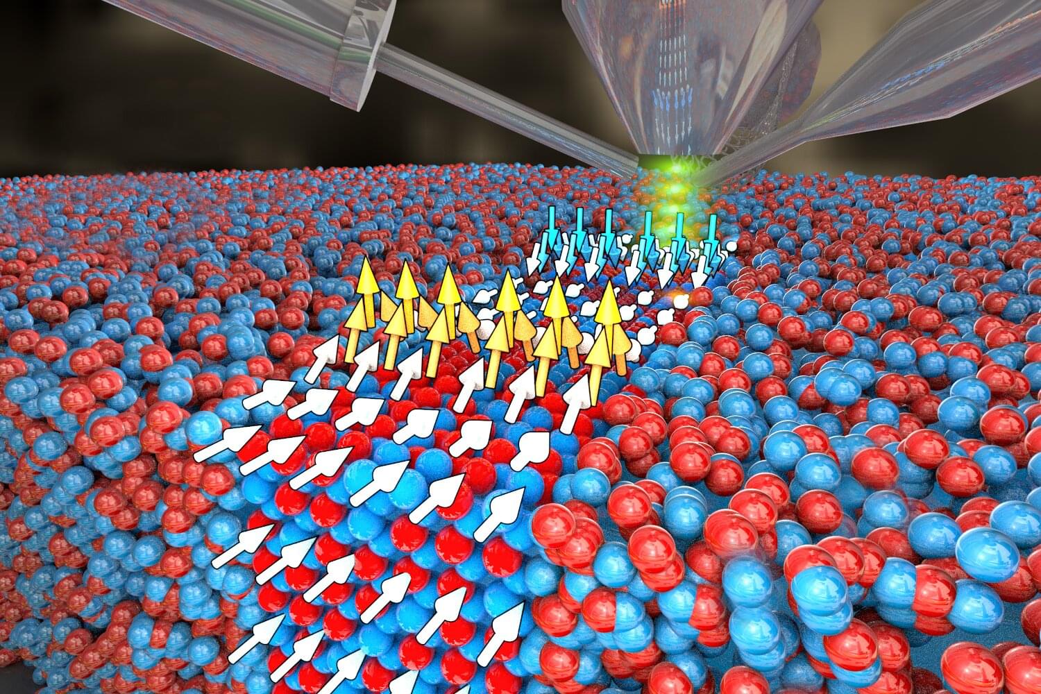
Researchers at HZDR have partnered with the Norwegian University of Science and Technology in Trondheim, and the Institute of Nuclear Physics in the Polish Academy of Sciences to develop a method that facilitates the manufacture of particularly efficient magnetic nanomaterials in a relatively simple process based on inexpensive raw materials.
Using a highly focused ion beam, they imprint magnetic nanostrips consisting of tiny, vertically aligned nanomagnets onto the materials. As the researchers have reported in the journal Advanced Functional Materials, this geometry makes the material highly sensitive to external magnetic fields and current pulses.
Nanomagnets play a key role in modern information technologies. They facilitate fast data storage, precise magnetic sensors, novel developments in spintronics, and, in the future, quantum computing. The foundations of all these applications are functional materials with particular magnetic structures that can be customized on the nanoscale and precisely controlled.

Scientists from the Indian Institute of Technology Bombay have found a way to use light to control and read tiny quantum states inside atom-thin materials. The simple technique could pave the way for computers that are dramatically faster and consume far less power than today’s electronics.
The materials studied are just one atom thick—far thinner than a human hair—and are known as two-dimensional (2D) semiconductors. Inside these materials, electrons can sit in one of two distinct quantum states, called valleys. These valleys, named K and K′, can be thought of as two different “locations” that an electron can choose between. Because there are two options, researchers have long imagined using them like the 0 and 1 of digital computing, but on a quantum level. This idea is the foundation of a rapidly growing research field called valleytronics.
However, being able to reliably control which valley electrons occupy—and to switch between them quickly and on demand—has been a major challenge. “Previous methods required complicated experimental setups with carefully tuned circularly polarized lasers and often multiple laser pulses, and they only worked under specific conditions,” said Prof. Gopal Dixit.

Diamond is famous in material science for being the best natural heat conductor on Earth—but new research reveals that, at the atomic scale, it can briefly trap heat in unexpected ways. The findings could influence how scientists design diamond-based quantum technologies, including ultra-precise sensors and future quantum computers.
In a study published in Physical Review Letters, researchers from the University of Warwick and collaborators showed that when certain molecular-scale defects in diamond are excited with light, they create tiny, short-lived “hot spots” that momentarily distort the surrounding crystal. These distortions last only a few trillionths of a second but are long enough to affect the behavior of quantum-relevant defects.
“Finding a hot ground state for a molecular-scale defect in diamond was extremely surprising for us,” explained Professor James Lloyd-Hughes, Department of Physics, University of Warwick. “Diamond is the best thermal conductor, so one would expect energy transport to prevent any such effect. However, at the nanoscale, some phonons—packets of vibrational energy—hang around near the defect, creating a miniature hot environment that pushes on the defect itself.”
Researchers at the Paul Scherrer Institute PSI, in collaboration with the National Institute of Standards and Technology (NIST) in Boulder, Colorado, have for the first time succeeded in using existing laser technology to continuously vary the magnetic properties of two-dimensional materials.
This simple and fast method should make a large number of applications possible, including techniques for data storage and processing. The work is published in the journal Nature Communications.
Sometimes using conventional tools in a novel way produces astounding results. That’s what happened when researchers used the high-tech laser equipment in PSI’s cleanroom for something it was not intended to do. It was originally purchased for photolithography—a process for producing tiny 2D structures.

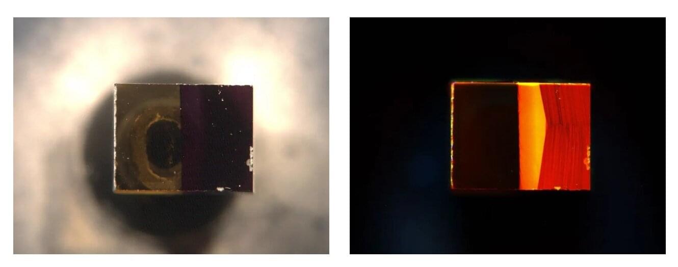
Researchers from TU Delft and Radboud University (The Netherlands) have discovered that the two-dimensional ferroelectric material CuInP₂S₆ (CIPS) can be used to control the pathway and properties of blue and ultraviolet light like no other material can.
With ultraviolet light being the workhorse of advanced chipmaking, high-resolution microscopy and next-generation optical communication technologies, improving the on-chip control over such light is vital. As the researchers describe in the journal Advanced Optical Materials, CIPS can be integrated onto chips, opening exciting new avenues for integrated photonics.