Toggle light / dark theme

Prof Lee said, “Existing breakthrough studies in quantum advantage are limited to highly-specific tailored problems. Finding new applications for which quantum computers provide unique advantages is the central motivation of our work.”

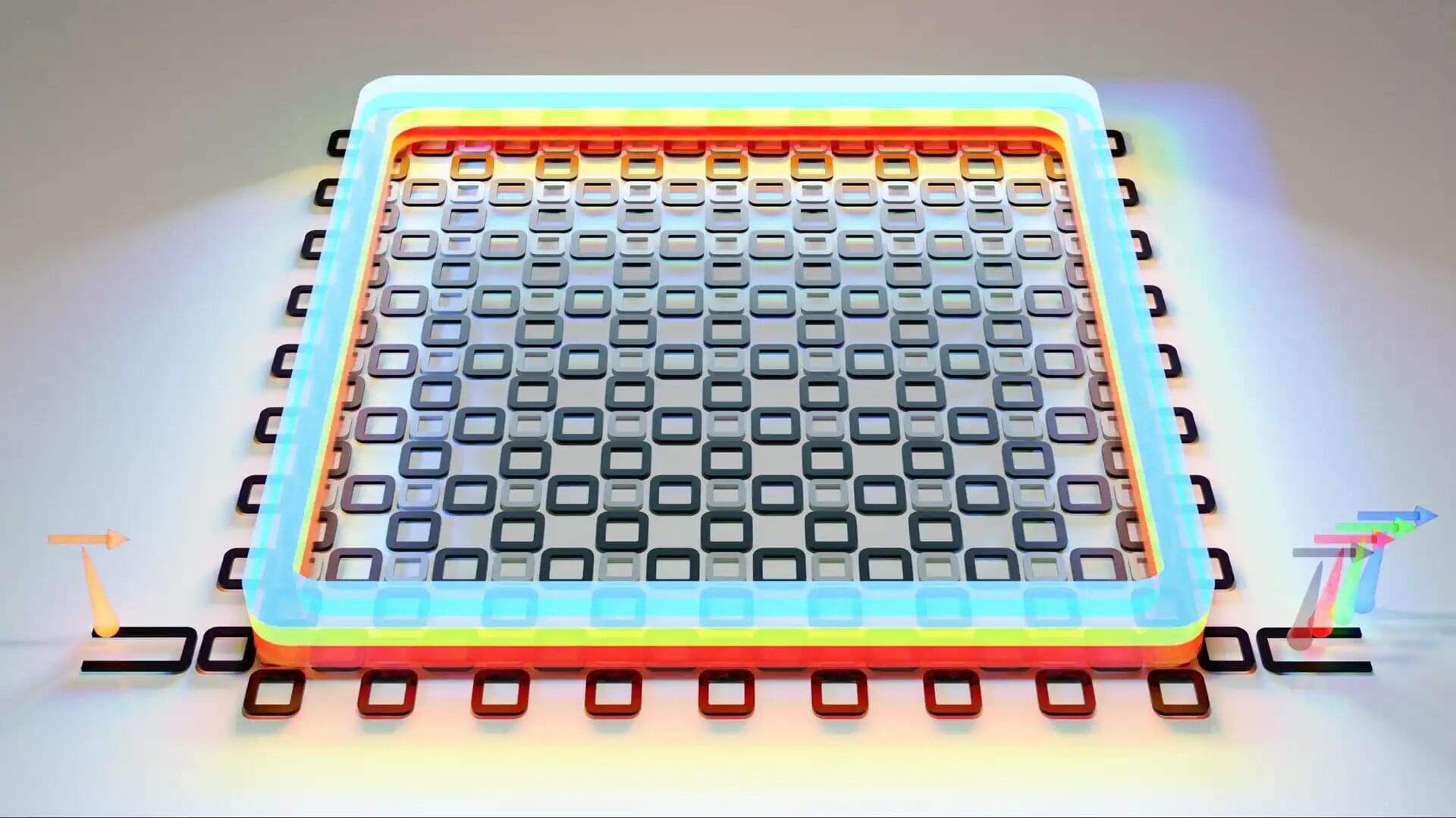
“Our approach allows us to explore the intricate signatures of topological materials on quantum computers with a level of precision that was previously unattainable, even for hypothetical materials existing in four dimensions,” added Prof Lee.

Despite the limitations of current noisy intermediate-scale quantum (NISQ) devices, the team is able to measure topological state dynamics and protected mid-gap spectra of higher-order topological lattices with unprecedented accuracy, thanks to advanced in-house developed error mitigation techniques. This advance demonstrates the potential of current quantum technology to explore new frontiers in material engineering.

It’s not easy making green.

For years, scientists have fabricated small, high-quality lasers that generate red and blue light. However, the method they typically employ — injecting electric current into semiconductors — hasn’t worked as well in building tiny lasers that emit light at yellow and green wavelengths. Researchers refer to the dearth of stable, miniature lasers in this region of the visible-light spectrum as the “green gap.” Filling this gap opens new opportunities in underwater communications, medical treatments and more.

Compact laser diodes can emit infrared, red and blue wavelengths, but are highly inefficient at producing green and yellow wavelengths, a region known as the ‘green gap’. (Image: S. Kelley, NIST)

Neuralink’s first patient says he’s given his brain-chip implant a name seven months after it was surgically implanted.

Noland Arbaugh, who is quadriplegic and became the first person to get the computer-controlling implant developed by Elon Musk’s brain-interface company, said Wednesday that he had named the device “Eve” and was working with it to improve himself in different ways.

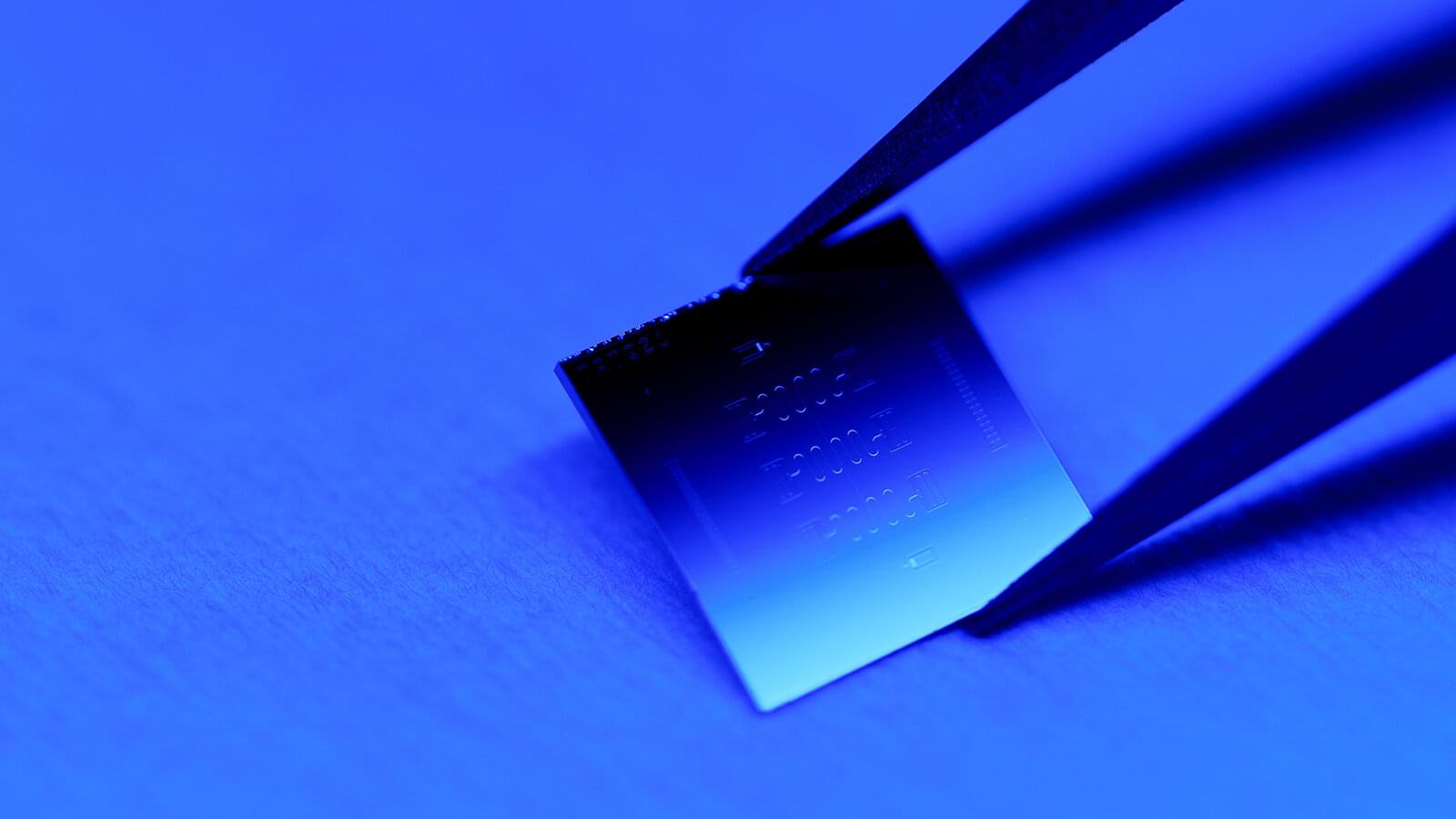
A recent study led by University of Minnesota Twin Cities researchers provides fundamental insight into how light, electrons, and crystal vibrations interact in materials. The research has implications for developing on-chip architectures for quantum information processing, significantly reducing fabrication constraints, and thermal management.

Researchers have engineered a new technique to trap ions in 3D structures using modified electric fields in Penning traps, forming stable bilayer crystals.

This innovation paves the way for more complex quantum devices and could revolutionize quantum computing and sensing by utilizing space more efficiently.

Quantum Device Challenges

Scientists at the Princeton Plasma Physics Laboratory are pioneering the use of liquid lithium in spherical tokamaks to enhance fusion performance.

Recent computer simulations suggest the optimal placement of lithium vapor to protect the tokamak’s interior from intense plasma heat. Innovative configurations, such as the lithium “cave” and porous plasma-facing walls, aim to simplify the design and improve heat dissipation, contributing to the future of fusion energy.

Inside the next generation of fusion vessels known as spherical tokamaks, scientists at the U.S. Department of Energy’s Princeton Plasma Physics Laboratory (PPPL) envisioned a hot region with flowing liquid metal that is reminiscent of a subterranean cave. Researchers say evaporating liquid metal could protect the inside of the tokamak from the intense heat of the plasma. It’s an idea that dates back several decades and is tied to one of the Lab’s strengths: working with liquid metals.

A team of researchers has developed a novel computational imaging system designed to address the challenges of real-time monitoring in ultrafast laser material processing. The new system, known as Dual-Path Snapshot Compressive Microscopy (DP-SCM), represents a significant advancement in the field, offering unprecedented capabilities for high-speed, high-resolution imaging. The team was led by Yuan Xin from Westlake University and Shi Liping from Xidian University.

The tin-vacancy center in diamond has properties that could be useful for quantum networks.

In a new study, researchers show how this defect’s electron spin can be controlled — and coherence prolonged — using a superconducting microwave waveguide.


Even the most pristine diamonds can host defects arising from missing atoms (vacancies) or naturally occurring impurities. These defects possess atomlike properties such as charge and spin, which can be accessed optically or magnetically. Over the past few decades, researchers have studied various defects to understand and harness these properties. One in particular—the tin-vacancy center, in which a tin atom resides on an interstitial site with two neighboring vacancies—exhibits exceptionally useful optical and spin properties, making it highly relevant in the field of quantum communication. Here, we explore how the spin properties behave under different magnetic field directions.

We demonstrate that manipulating electron spins is more straightforward in strained diamonds, as the electron spin is more responsive to an alternating magnetic field. We use superconductors known for generating no heat when a current flows through them, ensuring that we do not negatively affect the spin properties.