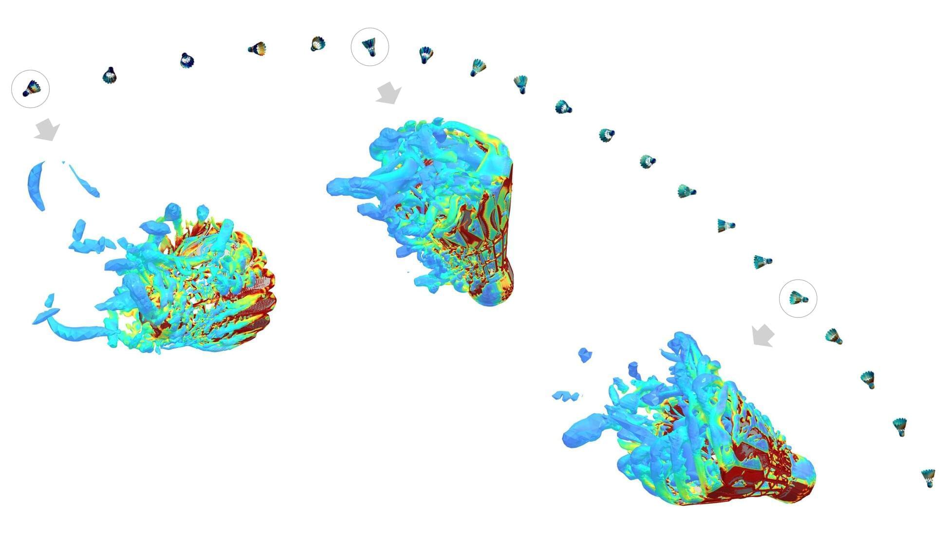
One of the world’s most popular sports, badminton is played by around 220 million people across the globe. As with other racket sports, a well-executed serve can establish a consequential advantage at the start of a rally.


Water-cooled computer mounted on wall brings steampunk art to life.
Billet Labs’ latest wall-mounted PC mod blends Victorian steampunk design with modern high-end hardware.


Caltech scientists have created a hybrid quantum memory that converts electrical information into sound, allowing quantum states to last 30 times longer than in standard superconducting systems.
Their mechanical oscillator, like a microscopic tuning fork, could pave the way for scalable and reliable quantum storage.
Quantum Bits vs. Classical Bits.

3D printing is a simple way to create custom tools, replacement pieces and other helpful objects, but it is also being used to create untraceable firearms, such as ghost guns, like the one implicated in the late 2024 killing of UnitedHealthcare CEO Brian Thompson.
Netanel Raviv, assistant professor of computer science & engineering in the McKelvey School of Engineering at Washington University in St. Louis, led a team from the departments of Computer Science & Engineering and Biomedical Engineering that has developed a way to create an embedded fingerprint in 3D-printed parts that would withstand the item being broken, allowing authorities to gain information for forensic investigation, such as the identity of the printer or the person who owns it and the time and place of printing.
The research will be presented at the USENIX Security Symposium Aug. 13–15, 2025, in Seattle. The first authors of the paper are Canran Wang and Jinweng Wang, who earned doctorates in computer science in 2024 and 2025, respectively. The research is published on the arXiv preprint server.


Terra Quantum has published a groundbreaking advance in quantum error correction that redefines how we scale quantum computing. In the peer-reviewed paper “QMM-Enhanced Error Correction: Demonstrating Reversible Imprinting and Retrieval for Robust Quantum Computation”, Terra Quantum scientists present QMM-Enhanced Error Correction, a hardware-validated, measurement-free method for suppressing quantum errors, based on principles derived initially from quantum gravity.
At the heart of this innovation is the Quantum Memory Matrix (QMM), a cosmology-inspired concept that models space-time as a lattice of finite-dimensional memory cells. Terra Quantum has now translated this deep theoretical idea into a functional quantum circuit. Validated on IBM’s superconducting processors, the QMM layer functions as a lightweight, unitary “booster” that enhances fidelity without mid-circuit measurements or added two-qubit gates, offering a powerful alternative to traditional surface codes.
“We have taken a concept rooted in quantum gravity and made it plug-and-play for today’s quantum processors,” said Florian Neukart, Chief Product Officer at Terra Quantum. “QMM-enhanced error correction works out of the box on existing hardware, requires no architectural changes, and delivers measurable gains. For industries building quantum solutions now, not in 10 years. This is a game-changer.
Terra Quantum has introduced QMM-Enhanced Error Correction, a hardware-validated, measurement-free method that suppresses quantum errors.

Researchers at the Johns Hopkins Applied Physics Laboratory (APL) in Laurel, Maryland, have demonstrated that a quantum algorithm can be used to speed up an information analysis task that classical computers struggle to perform.
The innovation tackles a key element of information operations: tracking and attributing topics and narratives as they emerge and evolve online, which can help analysts spot indications of potential terrorist acts, for example. This involves using computers to perform what’s known as semantic text similarity analysis, or comparing the similarities within a textual dataset — not just the similarity of the words, but the meaning behind them, which makes it possible to identify related texts even if they don’t share any common keywords.
“The amount of open-source text data online — on social media platforms especially — is growing dramatically, and our ability to analyze all of that data has not kept pace with our ability to collect it,” said Roxy Holden, a mathematician at APL and principal investigator of this effort. “Intelligence analysts have limited resources, so finding better ways to automate this kind of analysis is critical for the military and the intelligence community.”
APL researchers have demonstrated that a quantum algorithm can be used to speed up an information analysis task that classical computers struggle to perform.

Researchers at the Universitat Autònoma de Barcelona (UAB) have successfully created a new form of magnetic state known as a magneto-ionic vortex, or “vortion.” Their findings, published in Nature Communications, demonstrate an unprecedented ability to control magnetic properties at the nanoscale under normal room temperature conditions. This achievement could pave the way for next-generation magnetic technologies.
As the growth of Big Data continues, the energy needs of information technologies have risen sharply. In most systems, data is stored using electric currents, but this process generates excess heat and wastes energy. A more efficient approach is to control magnetic memory through voltage rather than current. Magneto-ionic materials make this possible by enabling their magnetic properties to be adjusted when ions are inserted or removed through voltage polarity changes. Up to now, research in this field has mainly focused on continuous films, instead of addressing the nanoscale “bits” that are vital for dense data storage.
At very small scales, unique magnetic behaviors can appear that are not seen in larger systems. One example is the magnetic vortex, a tiny whirlpool-like magnetic pattern. These structures play an important role in modern magnetic data recording and also have biomedical applications. However, once a vortex state is established in a material, it is usually very difficult to modify or requires significant amounts of energy to do so.
