Toggle light / dark theme

These 9 Incredible Images Are a Mind-Boggling Remind of How Far Technology Has Come

Sometimes, while waiting for quantum computers to become a thing, or complaining that your stupid laptop keeps dying on 5 percent battery, it’s easy to forget just how far technology has come over the past 50 years.

Sure, we can all list off a whole bunch of innovations that have changed the way the world works — the Internet, smartphones, radio telescopes — but it’s hard to really put that kind of change into perspective.

Thankfully, pictures often speak louder than words, and so below are nine photos that’ll make you stop and raise your *praise hand* emojis to the sky in honour of the scientists and engineers that have got us where we are today.

A Case for Neural Augmentation

Hopefully in the future, when somebody tells you they will be making an appointment with a surgeon for an augment, they will come back smarter. The world will be a better place for it.

Reprinted with permission from the author.

Eric C. Leuthardt, M.D., is a neurosurgeon who is currently a professor with the Department of Neurological Surgery and the Department of Biomedical Engineering at Washington University in St. Louis. He is Director of the Center for Innovation in Neuroscience and Technology and the Brain Laser Center. His work has yielded him numerous accolades as a scientist, a neurosurgeon, and an inventor. He was named one of the Top Young Innovators by MIT’s magazine Technology Review. The magazine names individuals under the age of 35 each year whose work in technology has global impact. In addition to numerous peer reviewed publications, Leuthardt has numerous patents on file with the U.S. Patent and Trademark Office for medical devices and brain computer interface technologies.

Breakthrough could triple the energy collected by solar to 60% efficiency

Current solar cells are able to convert into electricity around 20% of the energy received from the Sun, but a new technique has the potential to convert around 60% of it by funneling the energy more efficiently.

UK researchers can now ‘funnel’ electrical charge onto a chip. Using the atomically thin semiconductor hafnium disulphide (HfS2), which is oxidized with a high-intensity UV laser, the team were able to engineer an electric field that funnels electrical charges to a specific area of the chip, where they can be more easily extracted.

This method has the potential to harvest three times the energy compared with traditional systems. The researchers believe their breakthrough could result in solar panels, no bigger than a book, producing enough energy to power a family-sized house.

I Can’t Wait to Break Samsung’s First ‘Unbreakable’ Display

Samsung proudly announced today that its “unbreakable smartphone panel” has been certified by Underwriters Laboratories (UL). This means this ultra durable display is much closer to very profitable things like military and automotive contracts. But let’s be serious. Somebody’s gonna find a way to break this thing, and I hope it’s me.

The new display owes its anti-destructive tendencies to a couple of innovations. Samsung says that the OLED panel has “an unbreakable substrate.” (A substrate is basically the coating that holds the display’s organic material, cathodes, and diodes together.) Additionally, the Samsung display uses a flexible new type of plastic that won’t crack like glass. So you can supposedly drop it, smash it, and bend it without breaking the display.

Nanocrystals emit light

Using advanced fabrication techniques, engineers at the University of California San Diego have built a nanosized device out of silver crystals that can generate light by efficiently “tunneling” electrons through a tiny barrier. The work brings plasmonics research a step closer to realizing ultra-compact light sources for high-speed, optical data processing and other on-chip applications.

The work is published July 23 in Nature Photonics.

The device emits light by a quantum mechanical phenomenon known as inelastic electron tunneling. In this process, electrons move through a solid barrier that they cannot classically cross. And while crossing, the electrons lose some of their energy, creating either photons or phonons in the process.

Beyond silicon: $1.5 billion U.S. program aims to spur new types of computer chips

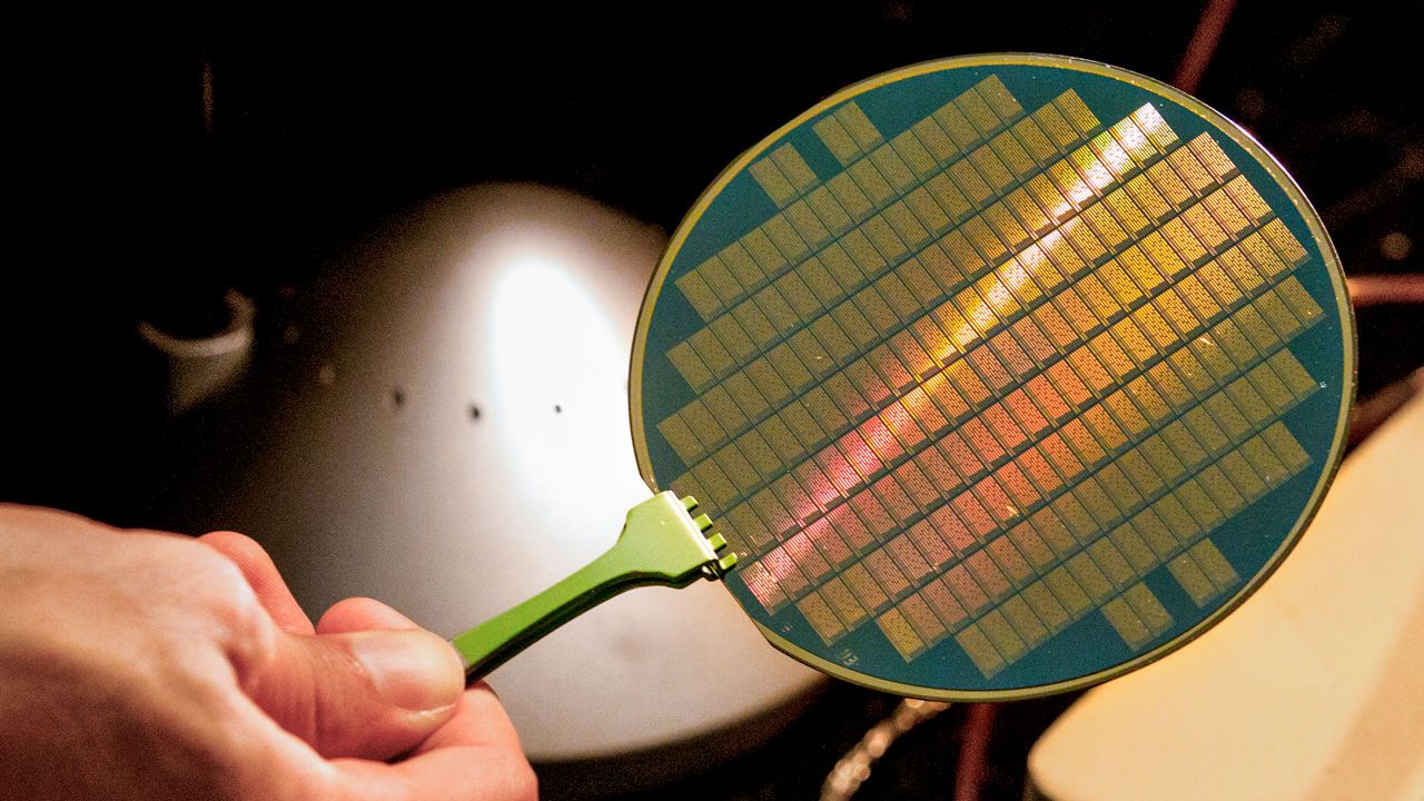
Silicon computer chips have been on a roll for half a century, getting ever more powerful. But the pace of innovation is slowing. Today the U.S. military’s Defense Advanced Research Projects Agency (DARPA) announced dozens of new grants totaling $75 million in a program that aims to reinvigorate the chip industry with basic research into new designs and materials, such as carbon nanotubes. Over the next few years, the DARPA program, which supports both academic and industry scientists, will grow to $300 million per year up to a total of $1.5 billion over 5 years.

“It’s a critical time to do this,” says Erica Fuchs, a computer science policy expert at Carnegie Mellon University in Pittsburgh, Pennsylvania.

In 1965, Intel co-founder Gordon Moore made the observation that would become his eponymous “law”: The number of transistors on chips was doubling every 2 years, a time frame later cut to every 18 months. But the gains from miniaturizing the chips are dwindling. Today, chip speeds are stuck in place, and each new generation of chips brings only a 30% improvement in energy efficiency, says Max Shulaker, an electrical engineer at the Massachusetts Institute of Technology in Cambridge. Fabricators are approaching physical limits of silicon, says Gregory Wright, a wireless communications expert at Nokia Bell Labs in Holmdel, New Jersey. Electrons are confined to patches of silicon just 100 atoms wide, he says, forcing complex designs that prevent electrons from leaking out and causing errors. “We’re running out of room,” he says.

/* */