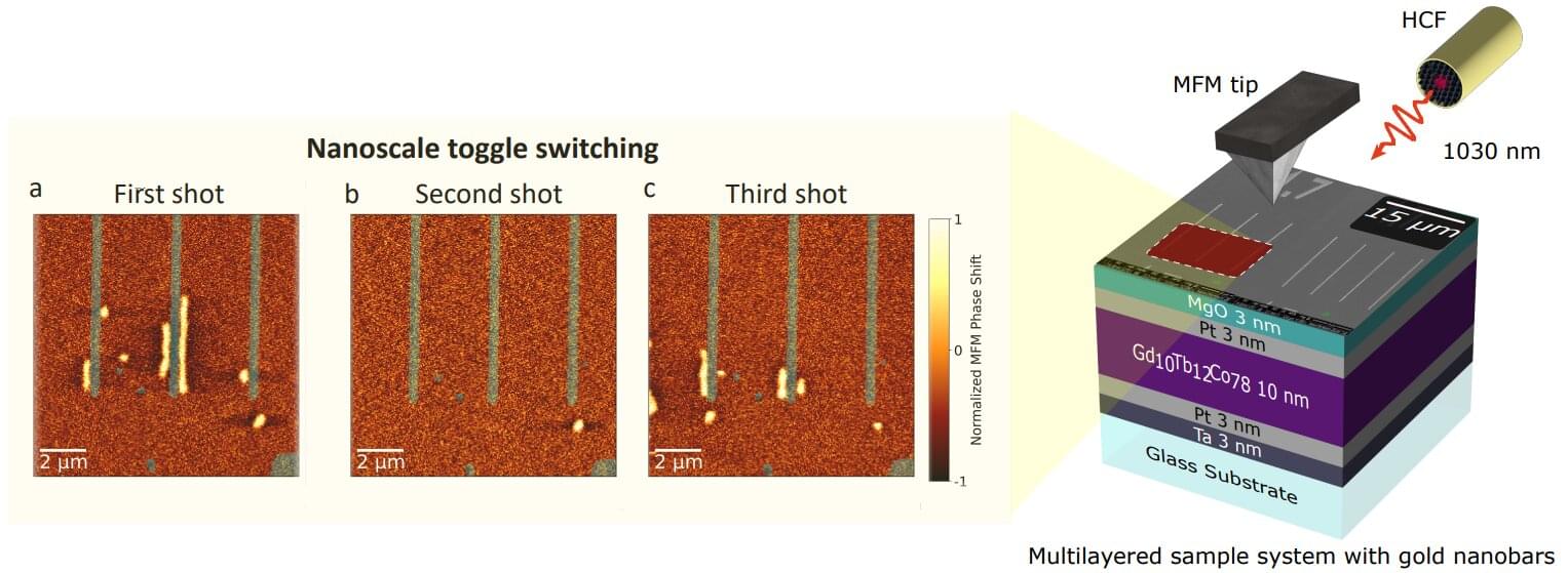
Researchers from Max Born Institute have demonstrated a successful way to control and manipulate nanoscale magnetic bits—the building blocks of digital data—using an ultrafast laser pulse and plasmonic gold nanostructures. The findings were published in Nano Letters.
All-optical, helicity-independent magnetization switching (AO-HIS) is one of the most interesting and promising mechanisms for this endeavor, where the magnetization state can be reversed between two directions with a single femtosecond laser pulse, serving as “0s” and “1s” without any external magnetic field or complex wiring. This opens up exciting possibilities for creating memory devices that are not only faster and more robust but also consume far less power.
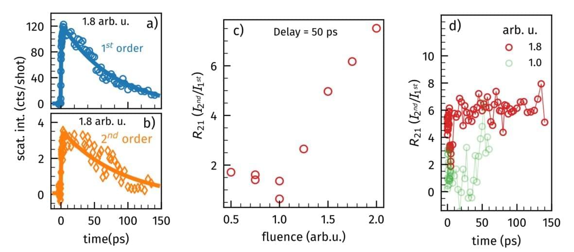
Ultrafast light-driven control of magnetization on the nanometer-length scale is key to achieving competitive bit sizes in next-generation data storage technology. However, it is currently not well understood to what extent basic physics processes such as heat transfer at the nanoscale and the propagation of magnetic domain walls limit the minimum achievable bit size.