Toggle light / dark theme

The things that can be done with 3D printing never cease to amaze. To the casual observer with only a passing knowledge of the technology, it appears on the surface to be an interesting method of producing plastic odds and ends, and sometimes metal parts – but 3D printing is so much more, as anyone who follows the progression of the technology on a regular basis knows. The things it is capable of producing are often hard to wrap one’s mind around – especially when you look at 3D printing on the nanoscale.

A group of scientists from Lithuania, France and Australia are busy studying 3D printing on a very small scale. As a newly published paper entitled “Optically Clear and Resilient Free-Form μ-Optics 3D-Printed via Ultrafast Laser Lithography” explains, 3D printing is capable of creating functional objects that are impossible to produce via conventional manufacturing techniques, and structures at the miniature, micro- and nanoscales are no exception.

Read more

Nice. I want one.


A revamped and rebranded NanoFabrication Kingston has launched with the goal of increasing activity outside of Queen’s University.

“We want to be open to the eastern Ontario community, industry and government as well as academia outside of Queen’s to make, characterize and test devices and samples that are small,” said Rob Knobel, Queen’s University professor and a lead researcher at NanoFabrication Kingston.

The lab’s basis is for the study and creation of innovations that require a scale of millionths of a millimetre.

In Brief:

  • Predictions from the co-chair of the World Economic Forum’s Future Council, Melanie Walker, say we’ll soon enter a post-hospital world due to advances in personalized medicine, health monitoring, and nanotechnology.
  • New and evolving technologies in medical science convince Walker we’ll live in a society not dependent on hospitals by 2030.

As the world of medicine is increasingly changed by biology, technology, communications, genetics, and robotics, predicting the outlook of the next few decades of medicine becomes harder. But that is exactly what Melanie Walker of the World Economic Forum does, and she predicts a bright new future for healthcare.

Read more

A simple technique for producing oxide nanowires directly from bulk materials could dramatically lower the cost of producing the one-dimensional (1D) nanostructures.

That could open the door for a broad range of uses in lightweight structural composites, advanced sensors, electronic devices – and thermally-stable and strong battery membranes able to withstand temperatures of more than 1,000 degrees Celsius.

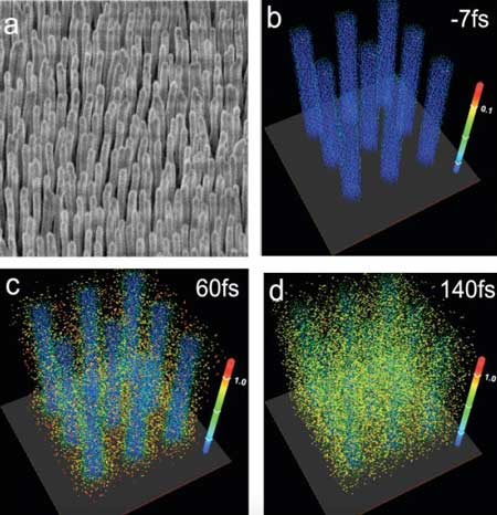
The technique uses a solvent reaction with a bimetallic alloy – in which one of the metals is reactive – to form bundles of nanowires (nanofibers) upon reactive metal dissolution.

Read more

Research by scientists at Swansea University is helping to meet the challenge of incorporating nanoscale structures into future semiconductor devices that will create new technologies and impact on all aspects of everyday life.

Dr Alex Lord and Professor Steve Wilks from the Centre for Nanohealth led the collaborative research published in Nano Letters. The research team looked at ways to engineer electrical contact technology on minute scales with simple and effective modifications to nanowires that can be used to develop enhanced devices based on the nanomaterials. Well-defined electrical contacts are essential for any electrical circuit and electronic device because they control the flow of electricity that is fundamental to the operational capability.

Everyday materials that are being scaled down to the size of nanometres (one million times smaller than a millimetre on a standard ruler) by scientists on a global scale are seen as the future of electronic devices. The scientific and engineering advances are leading to new technologies such as energy producing clothing to power our personal gadgets and sensors to monitor our health and the surrounding environment.

Read more

Australia getting their QC production lines ready with this advancement. BTW — get ready as the printers are coming soon.


The Australian National University (ANU) has led an international team to create a nano-sized diamond that’s harder than the natural gem and which will be useful for cutting through super-hard mining materials.

ANU Associate Professor Jodie Bradby said her team, including ANU PhD student Thomas Shiell and experts from RMIT, the University of Sydney and the United States, fabricated nano-sized Lonsdaleite, which is a hexagonal diamond only found in nature at meteorite impact sites, such as in Arizona’s Canyon Diablo.

‘This new diamond is not going to be on any engagement rings. You’ll more likely find it on a mining site, but I still think that diamonds are a scientist’s best friend,’ said Assoc Prof Bradby from the ANU Research School of Physics and Engineering.

Nice; ReRam with multi-state processing and reliable storage.


Short of full blown molecular computers or universal quantum computers or optical computers memristors have the most potential for a hardware change to dramatically boost the power and capabilities of computers. The boost to computer power could be nearly a million times by fully leveraging memristors. It would likely be more like a thousand times with more near to mid term usage of memristors.

Memristors (aka ReRAM) could become computer memory that is over 10 times denser than Flash or DRAM in two dimensions. Memristors like flash would be nonvolatile memory that would not need power for retain memory. Memristors are created from nanowire lattices which could be stacked in three dimensions. Memristors have also previously been shown to behave like brain synapses which could be used for computer architectures that emulate the human brain for neuromorphic computing. Now there is work on multistate memristors that perform computation. This means that eventually processing and memory could be tightly integrated.

Light travels 30 centimeters in 1 nanosecond. Wires have an approximate propagation delay of 1 ns for every 6 inches (15 cm) of length. Logic gates can have propagation delays ranging from more than 10 ns down to the picosecond range, depending on the technology being used.

Cracks sank the ‘unsinkable’ Titanic; decrease the performance of touchscreens and erode teeth. We are familiar with cracks in big or small three-dimensional (3D) objects, but how do thin two-dimensional (2D) materials crack? 2D materials, like molybdenum disulfide (MoS2), have emerged as an important asset for future electronic and photoelectric devices.

However, the mechanical properties of 2D materials are expected to differ greatly from 3D materials.

Scientists at the Center for Integrated Nanostructure Physics (CINAP), within the Institute for Basic Science (IBS) published, on Nature Communications (“Dynamical observations on the crack tip zone and stress corrosion of two-dimensional MoS2”), the first observation of 2D MoS2 cracking at the atomic level. This study is expected to contribute to the applications of new 2D materials.

Read more