Many of the previously dumb devices in our homes are getting smarter with the advent of internet-connected lights, thermostats, and more. Surely the windows can’t be smart, can they? A team of engineers from the German Friedrich-Schiller University Jena have created just that — a smart window that can alter its opacity and harvest energy from the sun’s rays.
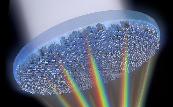
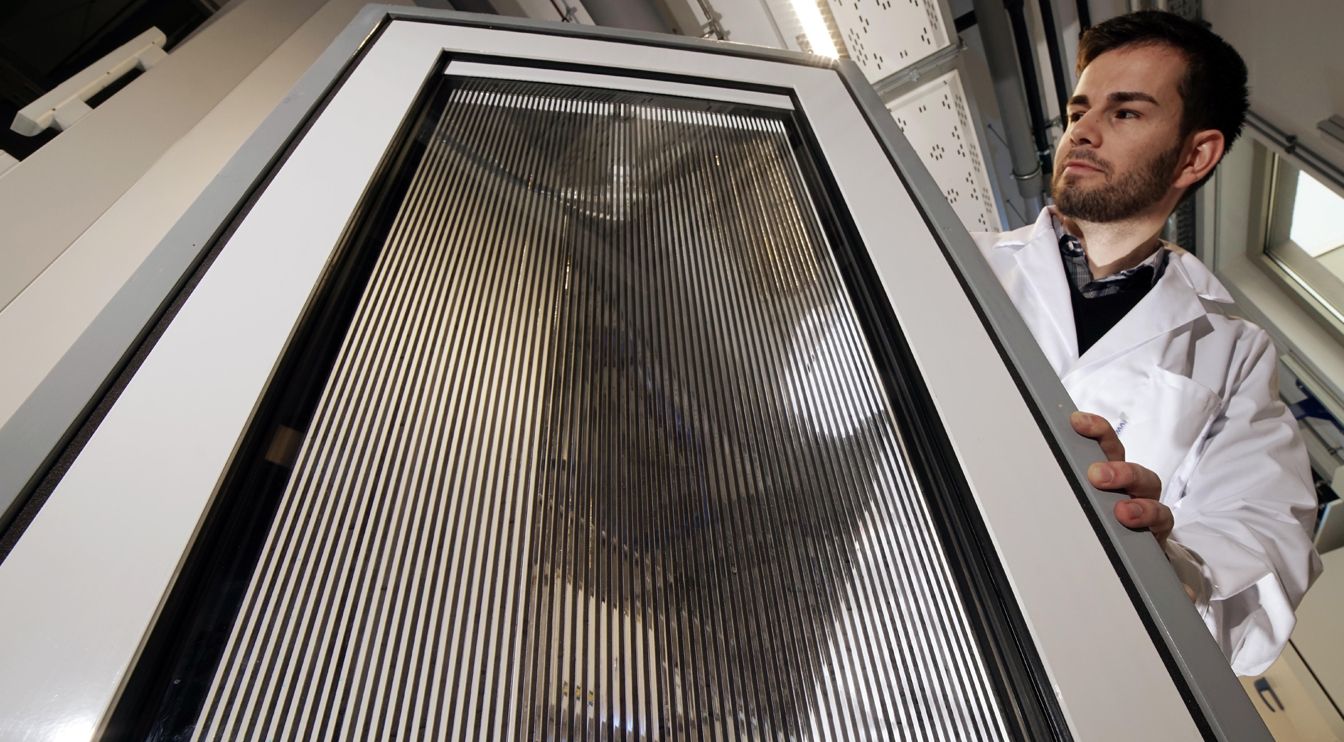
There have been a number of “smart” electrochromatic window designs over the years, but these are mostly aimed at changing tint or opacity only. The windows designed by Friedrich-Schiller University researchers are vastly more functional. The so-called Large-Area Fluidic Windows (LaWin) design uses a fluid suspension of iron particles. This fluid is contained within the window in a series of long vertical channels. These “functional fluids” allow the window to change opacity, but also absorb and distribute heat.
The iron-infused fluid remains diffused until you switch the window on — the nanoparticles cloud up the channels and block light. When you flip the switch, magnets drag the nanoparticles out of the liquid to make the window fully transparent. When the magnet is switched off, the nanoparticles are resuspended to darken the panel. In general, the more nanoparticles you add, the darker the window becomes. You can even completely black it out with enough iron.