Menu

Blog

Archive for the ‘nanotechnology’ category: Page 280

Mar 12, 2016

Interesting Nanotechnology Animation 2

Posted by in category: nanotechnology

Nanotech creates a non-stick bottle.

Read more

Mar 11, 2016

Ray Kurzweil says nanobots will connect your neocortex to the cloud

Posted by in categories: nanotechnology, neuroscience, Ray Kurzweil

Futurist Ray Kurzweil talks with StarTalk Radio’s Neil DeGrasse Tyson about the expansion of the human brain that he predicts will happen in the 2030’s.

Subscribe for more videos like this: http://bit.ly/1GpwawV

Continue reading “Ray Kurzweil says nanobots will connect your neocortex to the cloud” »

Mar 11, 2016

Digital CMOS Camera Series Boosts Quantum Efficiency (QE) For Breakthrough Photon Detection Capability

Posted by in categories: chemistry, nanotechnology, quantum physics, security

Digital CMOS camera with QE technology with improved photon detection capabilities — now this should interest to many medical departments, researchers, and even for security checkpoint screening.


Hamamatsu Corporation has again raised the bar in scientific CMOS camera performance with the 2016 version of the ORCA-Flash4.0 V2. The increased quantum efficiency (QE), now at a peak of 82%, increases the likelihood of detecting the faintest of signals, helping to answer the question “Is it there?” And, for brighter samples, higher QE translates into shorter exposure times without sacrificing image quality. The ORCA-Flash4.0 V2 opens up new possibilities for imaging in low conditions and improves signal to noise at all light levels.

Since its introduction and evolution, the ORCA-Flash4.0 series has become the favorite scientific CMOS camera of investigators everywhere, powering cutting-edge imaging research in every field from biology and chemistry to astrophysics and nanotechnology. The widespread appeal is due to the vast array of high-performance features: low read noise, large field of view, high dynamic range and fast frame rates. The newly enhanced QE of the “Flash V2” only serves to increase the power and versatility of this game-changing camera.

Continue reading “Digital CMOS Camera Series Boosts Quantum Efficiency (QE) For Breakthrough Photon Detection Capability” »

Mar 9, 2016

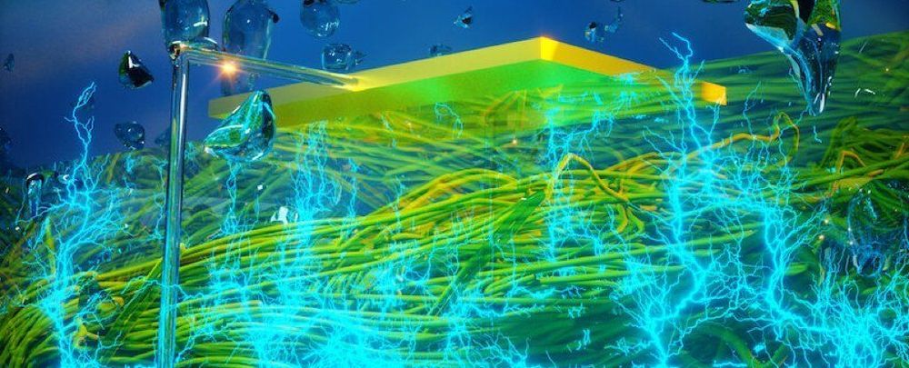
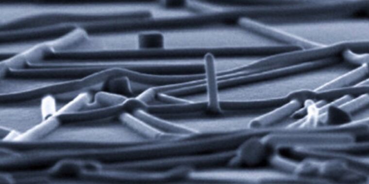
Chemists unravel their carbon ramen

Posted by in categories: chemistry, materials, nanotechnology

Noodle-like nanostructures emerge as a cheap alternative to graphene.

Read more

Mar 9, 2016

NIH awards grant to upstart for nanotech, regenerative spinal implants

Posted by in categories: biotech/medical, health, nanotechnology

New funding awarded by DARPA on new spinal implants; this should make some commercial pilots that I know happy.


Carmel, IN-based startup Nanovis is no stranger to nabbing research grants. It’s just nabbed one from the National Institutes of Health for preclinical research on the use of its porous Forticore interbody fusion devices in combination with nanotube technology. The combination is expected to result in a surface that mimics nature and encourages regeneration around an implant.

Nanovis has previously gotten 8 competitive peer-reviewed grants from the NIH and other research organizations; this is its second NIH grant. In September 2014, it got FDA clearance for its FortiCore interbody fusion devices and then last October it launched an expanded FortiCore line.

Continue reading “NIH awards grant to upstart for nanotech, regenerative spinal implants” »

Mar 9, 2016

Reconfigurable magnetic nanopatterns

Posted by in categories: computing, nanotechnology

Researchers in Milan have discovered which will lead to major improvements computing and sensing devices.


Scientists have demonstrated a novel approach for designing fully reconfigurable magnetic nanopatterns whose properties and functionality can be programmed and reprogrammed on-demand.

Read more

Mar 7, 2016

Newly developed model of DNA sheds light on molecule’s flexibility

Posted by in categories: bioengineering, biotech/medical, computing, genetics, nanotechnology

Knowledge of how DNA folds and bends could offer new perspective on how it is handled within cells while also aiding in the design of DNA-based nano-scale devices, says a biomedical engineer at Texas A&M University whose new motion-based analysis of DNA is providing an accurate representation of the molecule’s flexibility.

The model, which is shedding new light on the physical properties of DNA, was developed by Wonmuk Hwang, associate professor in the university’s Department of Biomedical Engineering, and his Ph.D. student Xiaojing Teng. Hwang uses computer simulation and theoretical analysis to study biomolecules such as DNA that carry out essential functions in the human body. His latest model, which provides a motion-based analysis of DNA is detailed in the scientific journal ACS Nano. The full article can be accessed at http://pubs.acs.org/doi/abs/10.1021/acsnano.5b06863.

In addition to housing the genetic information needed to build and maintain an organism, DNA has some incredibly interesting physical properties that make it ideal for the construction of nanodevices, Hwang notes. For example, the DNA encompassed within the nucleus of one human cell can extend to four feet when stretched out, but thanks to a number of folds, bends and twists, it remains in a space no bigger than one micron – a fraction of the width of a human hair. DNA also is capable of being programmed for self-assembly and disassembly, making it usable for building nano-mechanical devices.

Read more

Mar 4, 2016

The beginning of the end for encryption schemes? New quantum computer, based on five atoms, factors numbers in a scalable way

Posted by in categories: computing, education, encryption, nanotechnology, quantum physics

Replacing traditional encryption schemes.


What are the prime factors, or multipliers, for the number 15? Most grade school students know the answer — 3 and 5 — by memory. A larger number, such as 91, may take some pen and paper. An even larger number, say with 232 digits, can (and has) taken scientists two years to factor, using hundreds of classical computers operating in parallel.

Read more

Mar 1, 2016

Nanopatch polio vaccine success

Posted by in categories: bioengineering, biotech/medical, health, nanotechnology

Needle-free Nanopatch technology developed at The University of Queensland has been used to successfully deliver an inactivated poliovirus vaccine.

Delivery of a polio vaccine with the Nanopatch was demonstrated by UQ’s Professor Mark Kendall and his research team at UQ’s Australian Institute for Bioengineering and Nanotechnology, in collaboration with the World Health Organisation, the US Centres for Disease Control and Prevention, and vaccine technology company Vaxxas.

Professor Kendall said the Nanopatch had been used to administer an inactivated Type 2 poliovirus vaccine in a rat model.

Continue reading “Nanopatch polio vaccine success” »

Feb 29, 2016

Physicists promise a copper revolution in nanophotonics

Posted by in categories: computing, electronics, nanotechnology, physics

Researchers from the Moscow Institute of Physics and Technology (MIPT) have for the first time experimentally demonstrated that copper nanophotonic components can operate successfully in photonic devices – it was previously believed that only gold and silver components could do so. Copper components are not only just as good as components based on noble metals; they can also be easily implemented in integrated circuits using industry-standard fabrication processes. “This is a kind of revolution – using copper will solve one of the main problems in nanophotonics,” say the authors of the paper. The results have been published in the scientific journal Nano Letters.

The discovery, which is revolutionary for photonics and the computers of the future, was made by researchers from the Laboratory of Nanooptics and Plasmonics at MIPT’s Centre of Nanoscale Optoelectronics. They have succeeded, for the first time, in producing copper nanophotonic components, whose characteristics are just as good as those of gold components. It is interesting to note that the scientists fabricated the copper components using the process compatible with the industry-standard manufacturing technologies that are used today to produce modern . This means that in the very near future copper nanophotonic components will form a basis for the development of energy-efficient light sources, ultra-sensitive sensors, as well as high-performance optoelectronic processors with several thousand cores.

The discovery was made under what is known as nanophotonics – a branch of research which aims, among other things, to replace existing components in data processing devices with more modern components by using photons instead of electrons. However, while transistors can be scaled down in size to a few nanometres, the diffraction of light limits the minimum dimensions of photonic components to the size of about the light wavelength (~1 micrometre). Despite the fundamental nature of this so-called , one can overcome it by using metal-dielectric structures to create truly nanoscale photonic components. Firstly, most metals show a negative permittivity at optical frequencies, and light cannot propagate through them, penetrating to a depth of only 25 nanometres. Secondly, light may be converted into surface plasmon polaritons, surface waves propagating along the surface of a metal. This makes it possible to switch from conventional 3D photonics to 2D surface plasmon photonics, which is known as plasmonics. This offers the possibility of controlling light at a scale of around 100 nanometres, i.e., far beyond the diffraction limit.

Continue reading “Physicists promise a copper revolution in nanophotonics” »